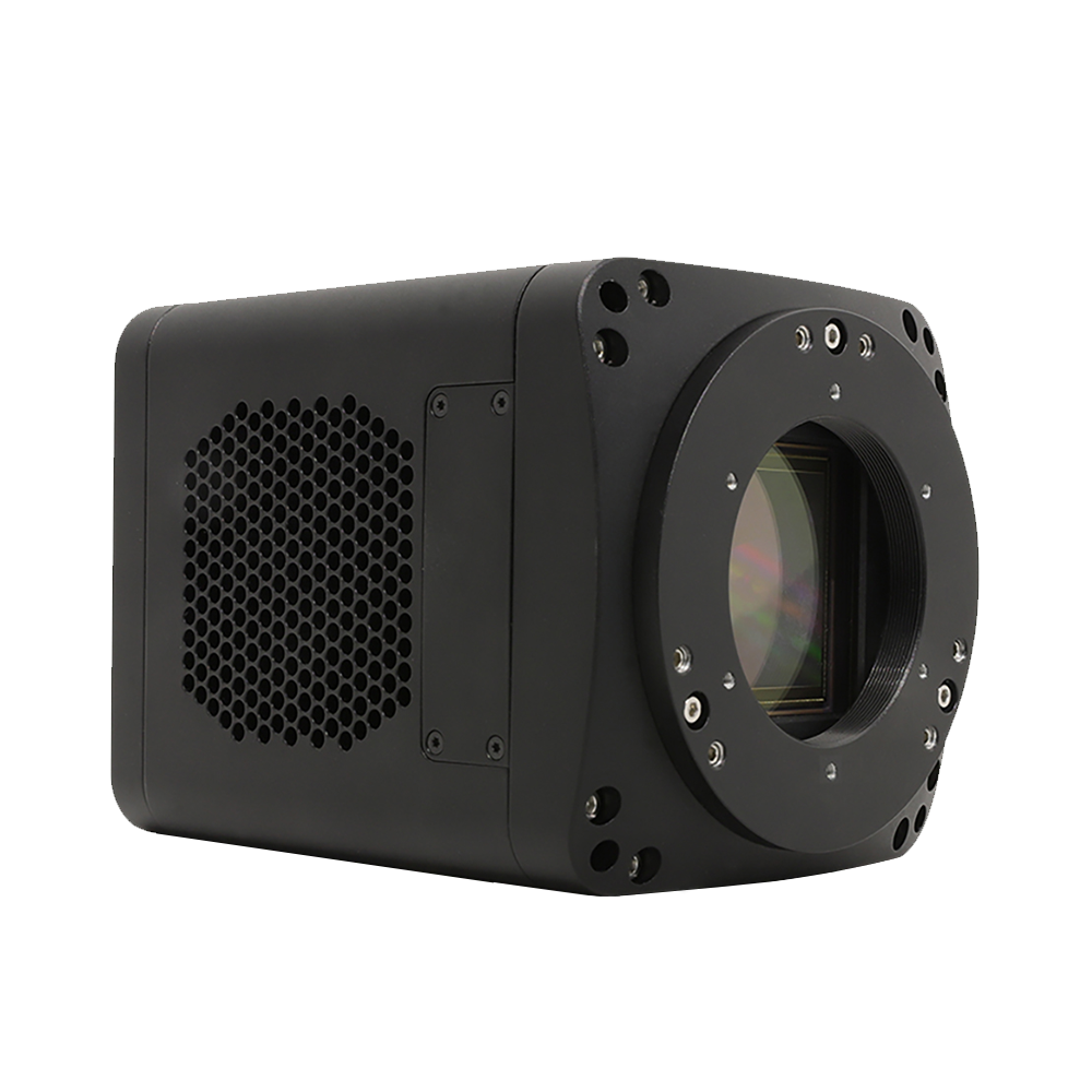
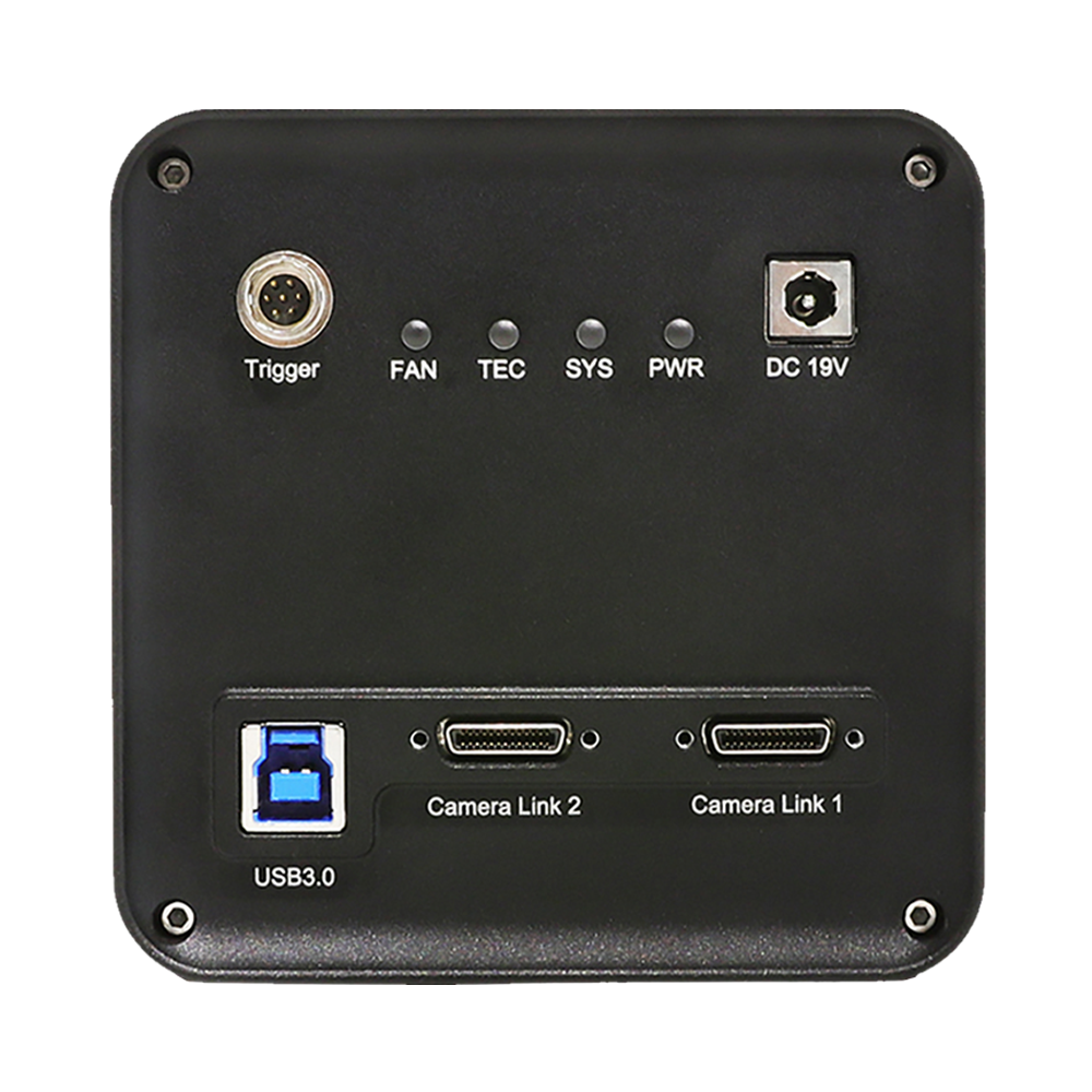
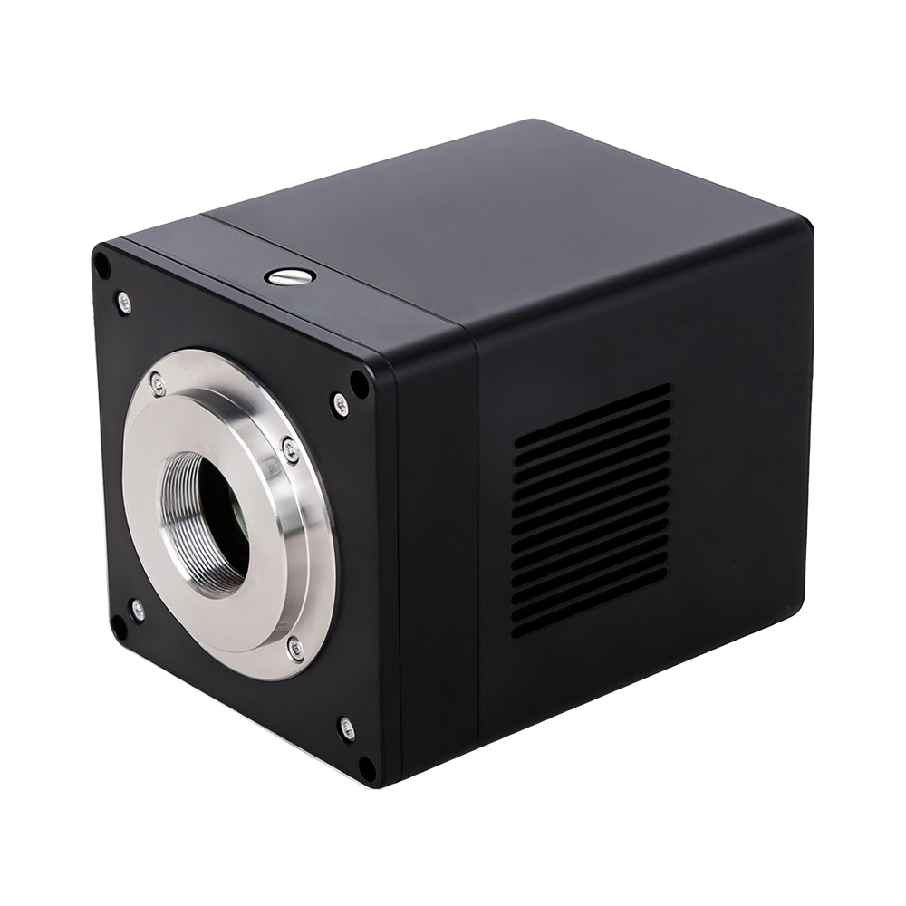
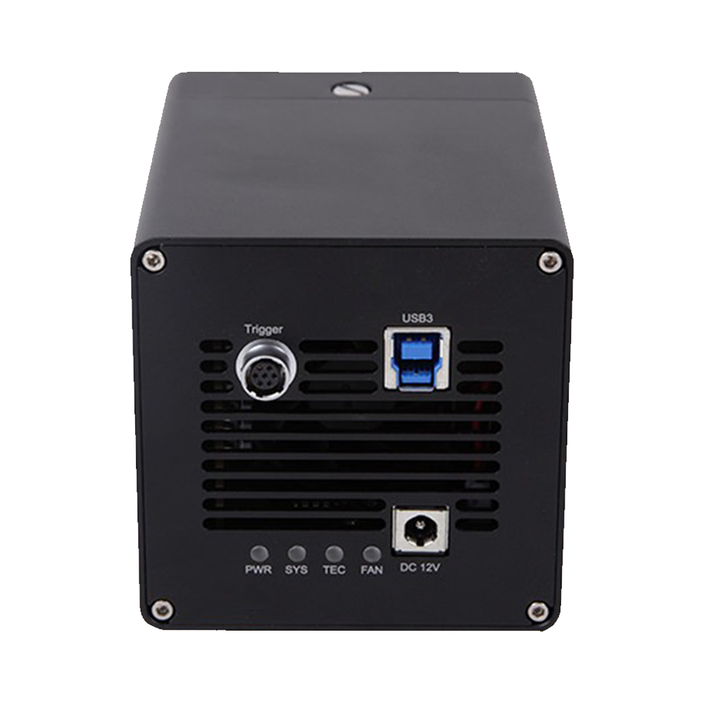
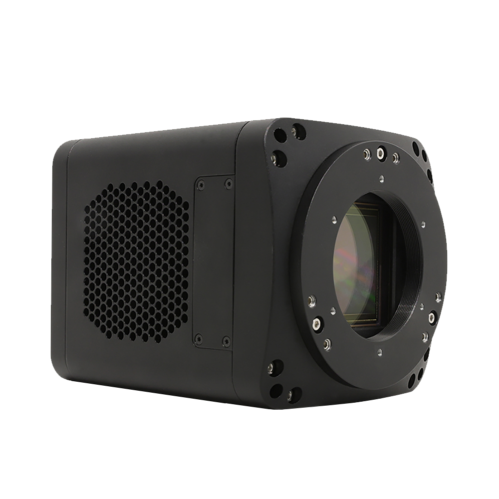
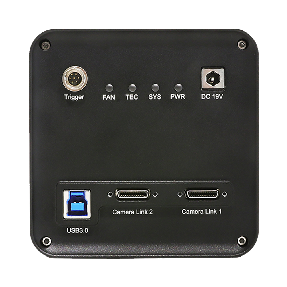
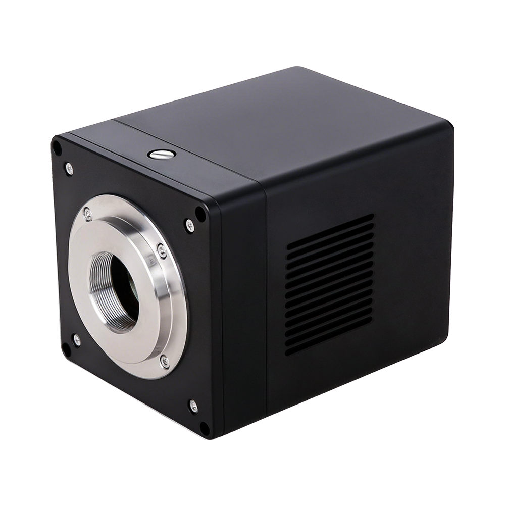
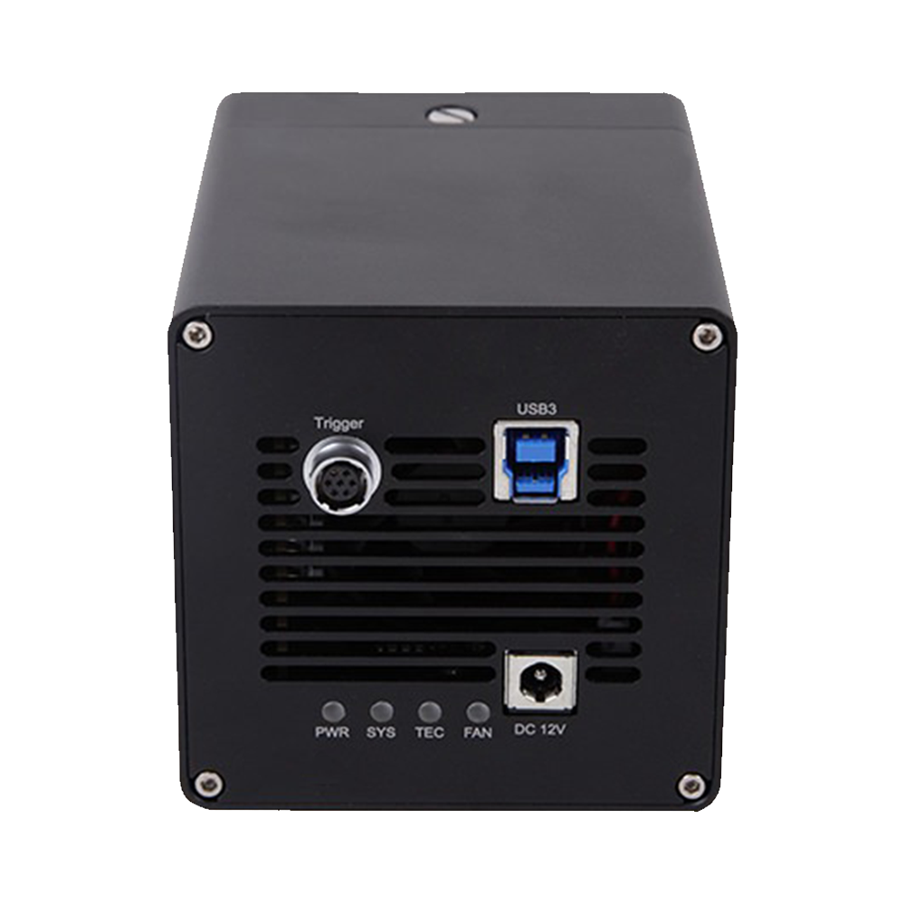
SR557MMA 科学相机
产品介绍
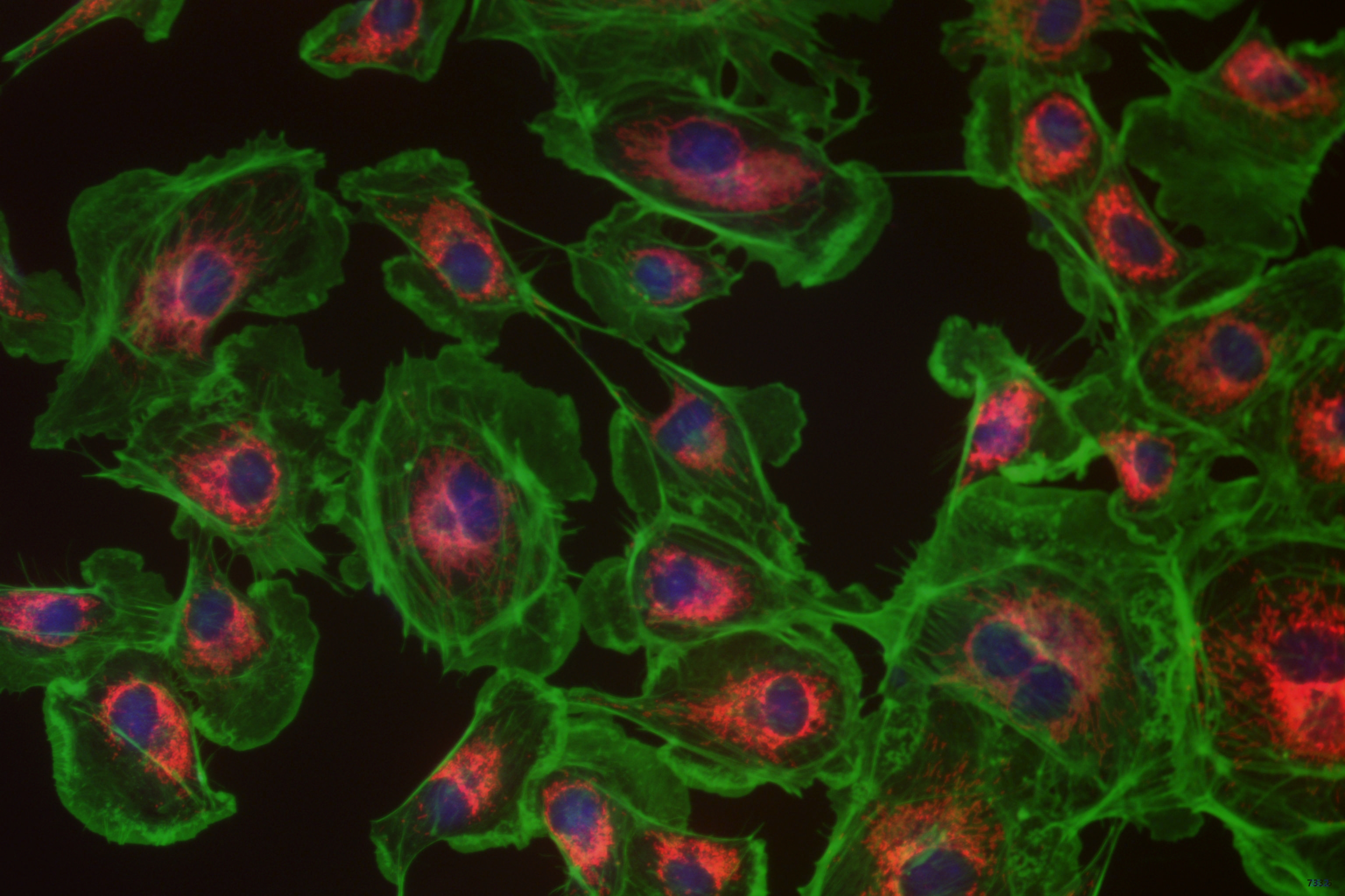
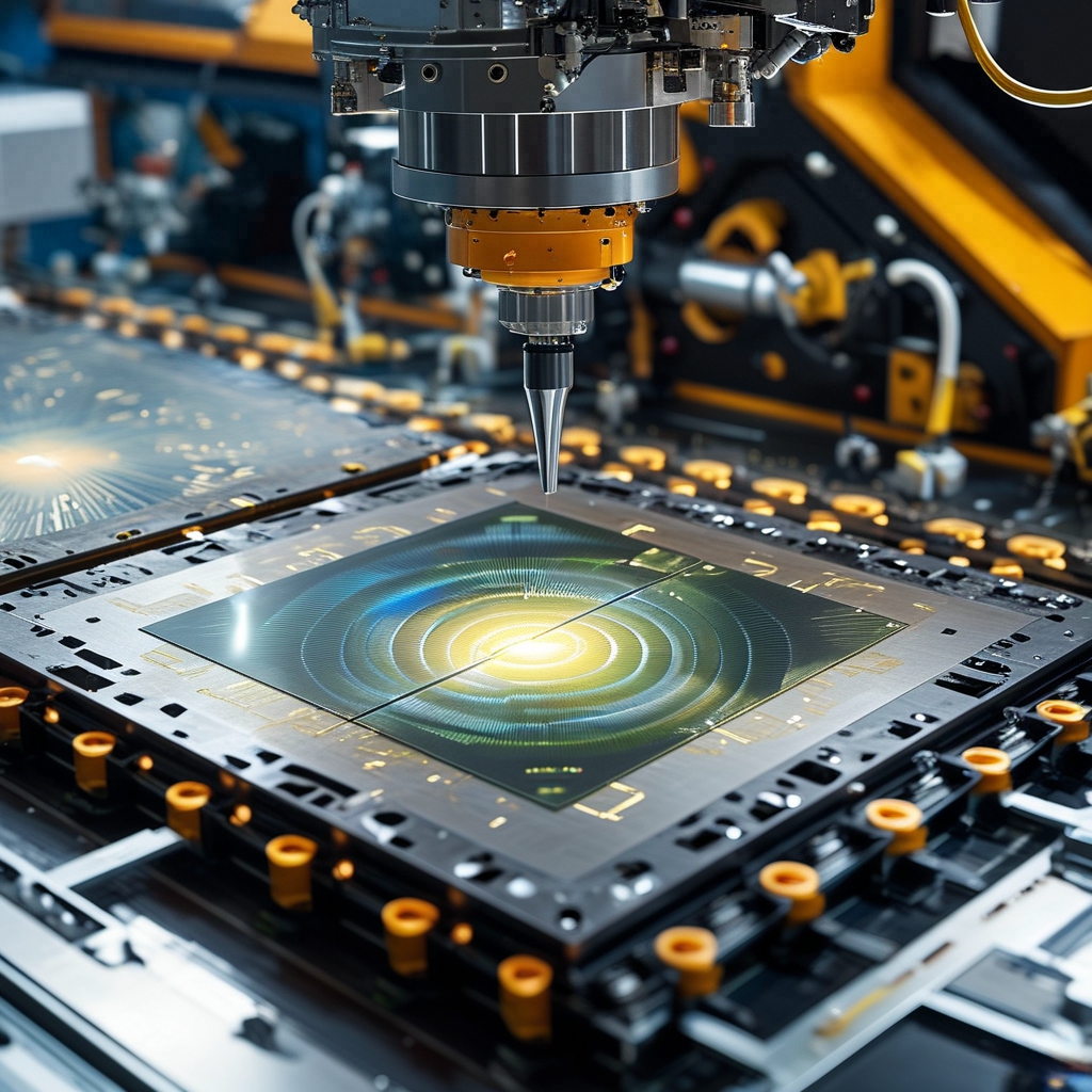
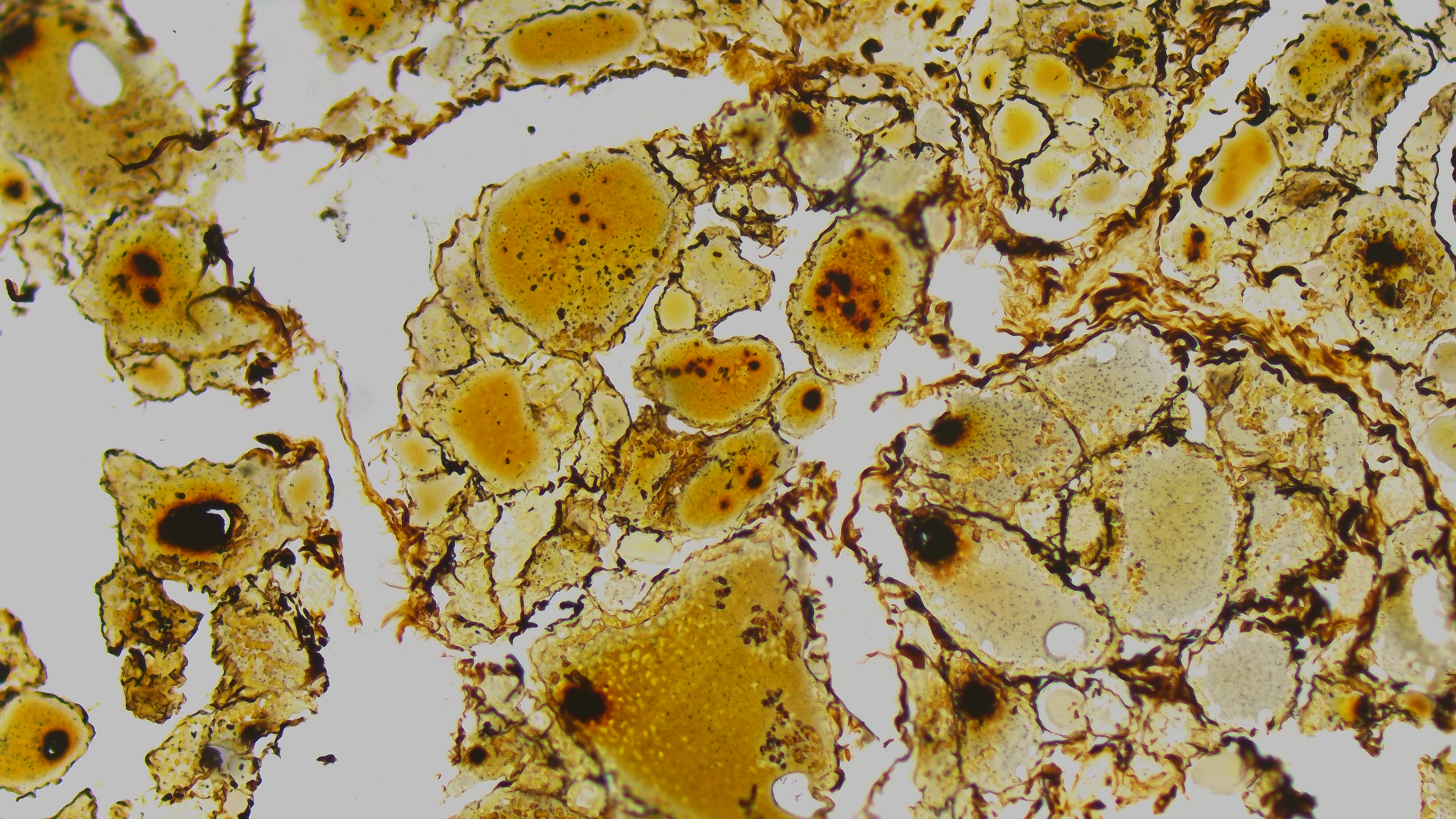
SR557MMA采用VPS2163A传感器,提供业界领先的557.1百万像素(20480×27200)超高分辨率成像能力。该型号专为需要极致细节捕捉的应用而设计,包括细胞形态学研究、生物组织全景成像、半导体晶圆缺陷检测和微结构精密测量。0.5微米的超小像元尺寸确保了在有限视野内捕获最大信息量,而TEC制冷系统有效控制了长时间采集的热噪声。
产品特点
- 采用VPS2163A超高分辨率CMOS图像传感器
- 世界级分辨率:20480×27200(557.1百万像素)
- 超小像元尺寸:0.5µm×0.5µm
- 1.08英寸光学格式,靶面对角约17.0mm
- 卷帘快门设计,适合静态或准静态成像
- TEC制冷系统,制冷温差≥40°C
- 内置512MB (4Gb)高速缓存
- USB 3.0高速数据接口(5 Gbps)
- 支持8/10-bit数据输出格式
- 全分辨率帧间隔约6秒
- 支持软件2×2/3×3/4×4 binning
- 光耦隔离I/O接口,支持外部触发同步
- 多种镜头接口选择:C/F/M42
- 适用于细胞学、组织学和半导体检测
- 提供完整的Windows/Linux SDK支持
产品详情
| 规格参数 | |
| 型号 | SR557MMA |
| 传感器 | VPS2163A (sCMOS) |
| 快门类型 | 卷帘快门 |
| 色彩类型 | 黑白 |
| 分辨率 | 557.1MP (20480×27200) |
| 传感器尺寸 | 10.24mm × 13.6mm |
| 传感器对角线 | 1.1" (17.02mm) |
| 像素尺寸 | 0.5µm × 0.5µm |
| 性能参数 | |
| 帧率 | 0.17fps@20480×27200(≈6 s/帧) |
| 位深 | 8/10bit |
| 动态范围 | TBD |
| 灵敏度 | TBD |
| 接口参数 | |
| GPIO | 1×光耦隔离输入, 1×光耦隔离输出, 2×TTL可编程IO |
| 镜头接口 | C(1.1")/F/M42(依机型) |
| 数据接口 | USB 3.0(5 Gbps) |
| 电源供电 | 12V DC |
| 物理参数 | |
| 外形尺寸 | TBD |
| 重量 | TBD |
| 环境参数 | |
| 工作温度 | 0°C ~ +40°C(建议值,依热设计可调整) |
| 工作湿度 | 20%~80%(无冷凝) |
| 存储温度 | -40°C ~ +85°C |
| 存储湿度 | TBD |
| 其他参数 | |
| 操作系统 | Windows/Linux |
| 认证 | CE/FCC |
产品概述
SR557MMA 是一款搭载 VPS2163A (sCMOS) 背照式 sCMOS 图像传感器的科学级制冷相机,具有以下特征:
- 高分辨率成像:557.1MP (20480×27200) 分辨率,0.5µm × 0.5µm 像元尺寸,靶面尺寸为 10.24mm × 13.6mm
- 快门设计:采用卷帘快门设计,支持黑白成像,适用于荧光成像、光谱分析、基因测序等科研场景
- 高速数据传输:支持 USB 3.0(5 Gbps) 高速数据接口,最大帧率可达 0.17fps@20480×27200(≈6 s/帧),数据输出格式涵盖 8/10bit
- 优异动态范围:动态范围最高可达 TBD,灵敏度为 TBD
- 制冷系统:内置制冷系统,可将温度降低至环境以下 TBD,有效降低暗电流
- 丰富接口:支持 GPIO 接口,镜头接口为标准 C(1.1")/F/M42(依机型) 接口
- 紧凑设计:整机尺寸为 TBD,重量约为 TBD,供电为 12V DC
- 全平台支持:支持 Windows/Linux 系统,配套 ToupView 软件及跨平台 SDK,支持 C/C++、C#、Python 等主流开发语言
核心性能指标
帧率
0.17fps@20480×27200(≈6 s/帧)
分辨率
557.1MP (20480×27200)
科学成像特性
背照式传感器
采用背照式 sCMOS 传感器,量子效率更高,特别适合微弱光成像应用
制冷降噪
内置制冷系统有效降低暗电流和噪声,提升图像质量和信噪比
高灵敏度
灵敏度达到 TBD,满足科学成像的高精度要求
灵活控制
支持ROI、Binning、触发控制等功能,适应不同科研需求
SR557MMA 相机凭借其卓越的科学成像性能、稳定的制冷系统和丰富的接口配置,是科研院所、医疗机构和高端工业应用的理想选择,能够满足各种精密成像和分析需求。
常见问题解答
了解更多关于科学级CMOS相机的专业知识
- 超低读出噪声:sCMOS 读出噪声接近 1e⁻,远优于传统 CCD
- 高帧率:并行读出架构支持高达100fps或更高的帧速
- 宽动态范围:可同时成像亮暗区域,动态范围可达上万比一
- 大视野和高分辨率:适合高分辨率大视野成像需求
EMCCD 更适合极弱光或长曝光场合。
sCMOS 在高分辨率、高帧率且需要低噪声的应用中性价比更高。
产品深度介绍
sCMOS传感器架构
每个像素配备独立放大器和柱级ADC,可并行读出,实现高速、高信噪比成像。双增益通道与双ADC设计进一步提升动态范围和灵敏度。
低噪声 + 宽动态
典型 sCMOS 噪声 <2 e⁻(30fps),动态范围可达50,000:1,分别远超传统CCD。
快速读出与多用途
并行读出架构支持高帧率 (>100fps),适合高速事件捕获,如细胞运动、荧光寿命、等离子体变化等。
微弱光成像能力
背照式 sCMOS QE 可达 >95%,在UV至近红外范围表现出色,同步具备低固定纹噪、冷却可低至 –30 °C 用于天文观测等。
应用场景与系统价值
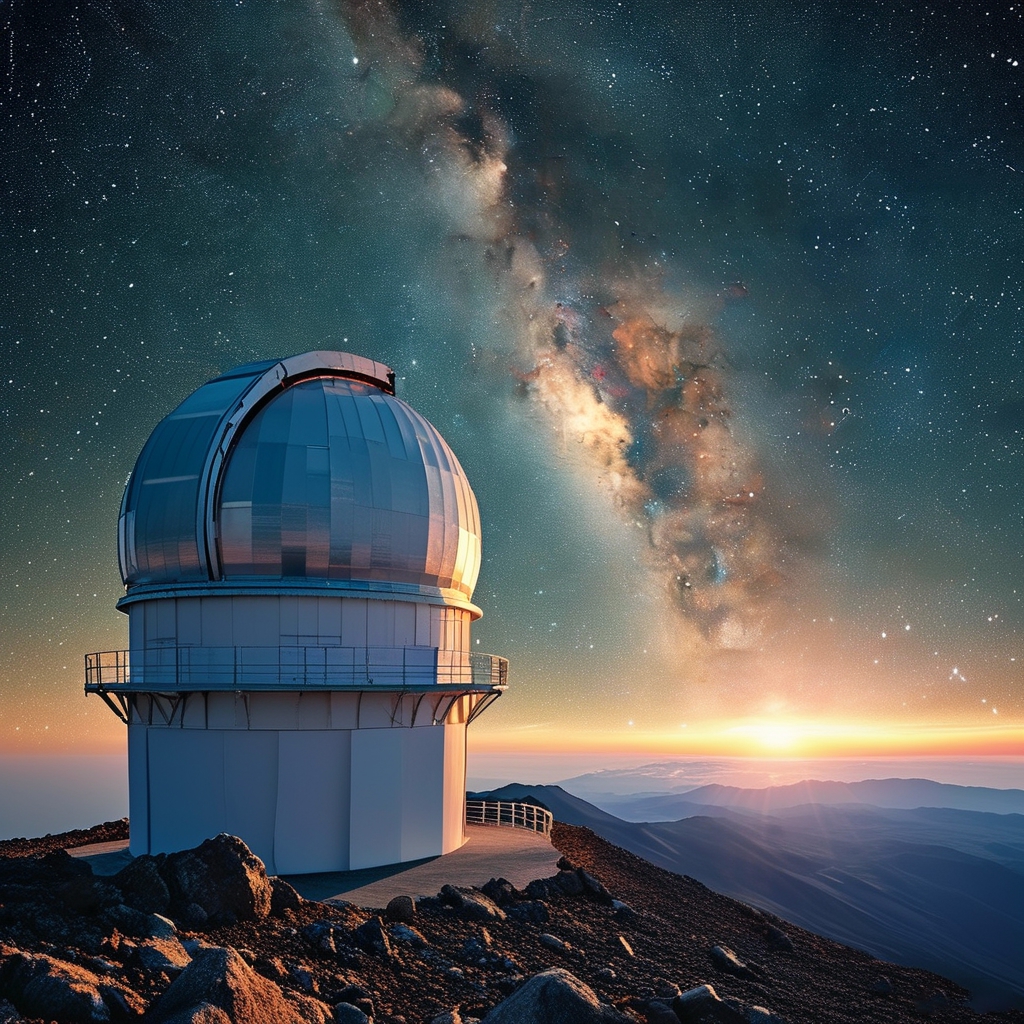
适合于荧光显微、天文成像、冷原子研究、X 射线成像、材料检测、工业显微等多个科研和行业领域,具有高灵敏度、高精度和高适应性的系统优势。